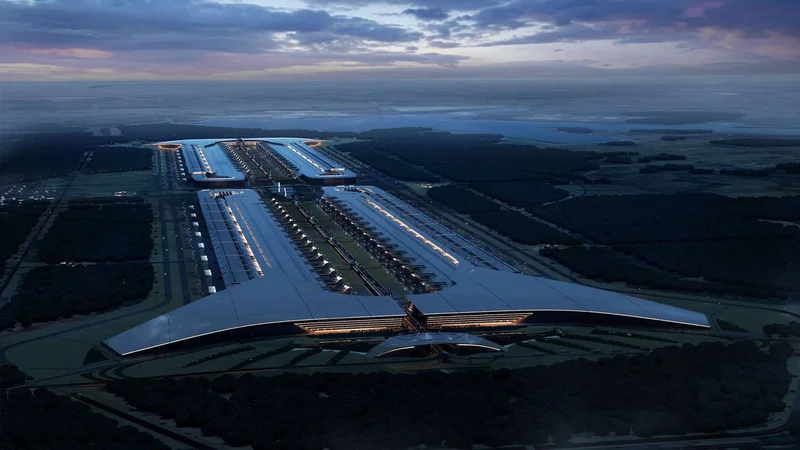
SpaceX and Tesla on Thursday formally unveiled plans for the initial phase of their Terafab project. The first stage of the plan — which is expected to use Intel's 14A process technology — is expected to require $16.8 billion in investment, while the completed campus is planned to encompass more than 100 million square feet of manufacturing space. The massive semiconductor manufacturing complex will be built in Grimes County, Texas, at a location that belongs to SpaceX.
According to SpaceX and Tesla, their combined demand for semiconductors is projected to exceed 1 terawatt (TW) of compute per year, which significantly exceeds today's global supply. In fact, SpaceX, Tesla, and xAI already consume a significant portion of contract chipmaking services available today, and can potentially justify building a dedicated fab that will exclusively serve Elon Musk's companies. In particular, Terafab is envisioned to exclusively produce AI inference processors for Tesla Optimus humanoid robots and Cybercab autonomous vehicles, as well as 'high-power' processors intended for SpaceX's space-based data centers. Meanwhile, SpaceX and Tesla have not disclosed when their combined demand for compute per year will hit the 1 TW benchmark.
Unlike a conventional semiconductor fab, Terafab is envisioned as a vertically integrated manufacturing campus where advanced logic devices, memory chips, packaging, and testing operations are housed together. Normally, logic and memory are produced at different fabs using different process technologies, whereas packaging and testing services are performed at different facilities. However, the companies believe that consolidating logic, memory, packaging, and testing in one location will not only shorten the production cycle but will also shorten time-to-yield by enabling faster iterative improvements.
Given the description and the goal of the project, this will be a massive facility. Yet, SpaceX and Tesla have said little about its capabilities; The only thing they have disclosed is that the current facility in Grimes County will feature '100 million square feet of manufacturing space.' The 100 million square feet (9.3 million square meters) figure immediately stands out because it is far beyond anything ever announced for a semiconductor manufacturing facility. For example, the total area of Samsung's Pyeongtaek campus is approximately 2.89 million square meters, or 31.1 million square feet. A single Samsung fab occupies about 120,000 square meters, or 1.29 million square feet. However, the key wording is important: '100 million square feet of manufacturing space' does not mean 100 million square feet of cleanroom space.
Based on an image published by SpaceX, the Terafab facility will occupy four massive buildings. It is unclear whether these buildings will be four phases of the project (i.e., logic, memory, and packaging will be made under one roof) or will serve different purposes (i.e., one building makes logic, another produces memory, yet another does testing and packaging). In any case, when fully built, Terafab will be a massive semiconductor production campus that will require significantly more than $16.8 billion.
The announcement claims that the Terafab facility will employ at least 3,000 people, and that between 60% and 80% of them will be Grimes and nearby Brazos County residents.
Terafab is expected to use water from Gibbons Creek Reservoir instead of local groundwater and feature on-site wastewater treatment as well as water recycling and conservation measures.
Get Tom's Hardware's best news and in-depth reviews, straight to your inbox.
The announcement follows Tesla's groundbreaking earlier this year on a research semiconductor facility at the North Campus of Tesla's Giga Texas campus, which the companies describe as a precursor to Terafab.
Anton Shilov is a contributing writer at Tom’s Hardware. Over the past couple of decades, he has covered everything from CPUs and GPUs to supercomputers and from modern process technologies and latest fab tools to high-tech industry trends.